
- NPN Transistor Definition: An NPN transistor is a widely used type of bipolar junction transistor, where a P-type semiconductor layer is flanked by two N-type layers.
- Symbol: The symbol for an NPN transistor shows the flow direction of the emitter current with an outward pointing arrow.
- Working Principle: The NPN transistor functions by allowing electrons to move from the emitter, through the base, to the collector, with the base current regulating this flow.
- Biasing Modes: It operates in three key modes: cut-off (no current flow), saturation (full current flow), and active (current amplification).
- Switch Capabilities: An NPN transistor can act as a switch, with the ability to turn on in saturation mode and off in cut-off mode.
What is a NPN Transistor
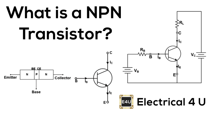
An NPN transistor is the most commonly used bipolar junction transistor, and is constructed by sandwiching a P-type semiconductor between two N-type semiconductors. An NPN transistor has three terminals– a collector, emitter and base. The NPN transistor behaves like two PN junctions diodes connected back to back.
These back to back PN junction diodes are known as the collector-base junction and base-emitter junction.
Regarding the three terminals of the NPN transistor, the Emitter is a region is used to supply charge carriers to the Collector via the Base region. The Collector region collects most of all charge carriers emitted from the Emitter. The Base region triggers and controls the amount of current flows through the Emitter to Collector.
The equivalent circuit of an NPN transistor is as shown in the figure below.

As a quick reminder, an N-type semiconductor is one where a large number of free electrons are available and it acts as a majority charge carrier. Under the influence of potential difference, electrons get sufficient energy and move from the valence band to the conduction band. Because of the movement of electrons, the current will flow through the N-type semiconductor.
Conversely, in P-type semiconductors, electrons are not available and hole acts as a majority charge carrier. Because of the movement of holes current will flow through the P-type semiconductor.
Construction of NPN Transistor
As discussed above, the NPN transistor has two junctions and three terminals. The construction of the NPN transistor is as shown in the below figure.

The emitter and collector layers are wider compared to the base. The emitter is heavily doped. Therefore, it can inject a large number of charge carriers to the base.
The base is lightly doped and very thin compared to the other two regions. It passes most of all charge carriers to the collector which is emitted by the emitter.
The collector is moderately doped and collects charge carriers from the base layer.
NPN Transistor Symbol
The symbol of the NPN transistor is as shown in the below figure. The arrowhead shows the conventional direction of Collector current (IC), Base current (IB) and Emitter current (IE).

How Does an NPN Transistor Work
The base-emitter junction is forward bias condition by the supply voltage VEE, while the collector-base junction is reverse biased by the supply voltage VCC.
In forward bias condition, the negative terminal of supply source (VEE) is connected to the N-type semiconductor (Emitter). Similarly, in a reverse bias condition, the positive terminal of the supply source (VCC) is connected to the N-type semiconductor (Collector).

The depletion region of the emitter-base region is thin compared to the depletion region of the collector-base junction (Note that the depletion region is a region where no mobile charge carriers are present and it behaves like a barrier that opposes the flow of the current).
In N-type emitter, the majority charge carrier is electrons. Therefore, electrons start flowing from N-type emitter to a P-type base. And because of electrons, the current will start flowing the emitter-base junction. This current is known as emitter current IE.
Electrons move into the base, a thin, lightly doped P-type semiconductor with limited holes for recombination. Therefore, most electrons bypass the base, with only a few recombining.
Because of the recombination, the current will flow through the circuit and this current is known as base current IB. The base current is very small compared to the emitter current. Typically, it is 2-5% of the total emitter current.
Most of the electrons pass the depletion region of a collector-base junction and pass through the collector region. The current flowing by the remaining electrons is known as the collector current IC. The collector current is large compared to the base current.
NPN Transistor Circuit
The circuit of the NPN transistor is as shown in the below figure.

The diagram shows how voltage sources are connected: the collector links to the positive terminal of VCC through a load resistance RL, which limits the maximum current flow.
The base terminal is connected to the positive terminal of base supply voltage VB with base resistance RB. The base resistance is used to limit the maximum base current.
When switched ON, the transistor allows a large collector current to flow, driven by a smaller base current entering the base terminal.
By KCL, the emitter current is the addition of base current and collector current.
![\[ I_E = I_B + I_C \]](https://www.electrical4u.com/wp-content/ql-cache/quicklatex.com-8bb6668aafa712bfce8c6f37d21e210f_l3.png "Rendered by QuickLaTeX.com")
Operating Mode of Transistor
The transistor operates on different modes or regions depends on the biasing of junctions. It has three modes of operation.
- Cut-off mode
- Saturation mode
- Active mode
Cut-off Mode
In cur-off mode, both junctions are in reverse bias. In this mode, the transistor behaves as an open circuit. And it will not allow the current to flow through the device.
Saturation Mode
In the saturation mode of a transistor, both junctions are connected in forward bias. The transistor behaves as a close circuit and current flow from collector to emitter when the base-emitter voltage is high.
Active Mode
In this mode of a transistor, the base-emitter junction is forward bias and collector-base junction is reverse biased. In this mode, the transistor operates as a current amplifier.
The current flows between emitter and collector and the amount of current are proportional to the base current.

NPN Transistor Switch
The transistor operates as switched ON in saturation mode and switched OFF in cut-off mode.
When both junctions are connected in the forward bias condition and sufficient voltage is given to input voltage. In this condition, collector-emitter voltage is near to zero and the transistor operates as a short circuit.
In this condition, the current will start flowing between collector and emitter. The value of the current flowing in this circuit is,
![\[ I_C = \frac{V_C_C}{R_C} \]](https://www.electrical4u.com/wp-content/ql-cache/quicklatex.com-949fb8a20e76c1ffc31f9847a63f9664_l3.png "Rendered by QuickLaTeX.com")

When both junctions are connected in reverse bias, the transistor behaves as an open circuit or OFF switch. In this condition, the input voltage or the base voltage is zero.
Therefore, the entire Vcc voltage appears across the collector. But, because of the reverse bias of the collector-emitter region, the current cannot flow through the device. Hence, it behaves as an OFF switch.
The circuit diagram of a transistor in the cut-off region is as shown in the below figure.

NPN Transistor Pinout
The transistor has three leads; collector (C), Emitter (E), and Base (B). In most of the configurations, middle lead is for Base.
To identify the emitter and collector pin, there is a dot on the surface of the SMD transistor. The pin which is exactly below this dot is a collector and the remaining pin is the emitter pin.
If the dot is not present, all pins will be placed with uneven space. Here middle pin is base. The closest pin of a middle pin is emitter and the remaining pin is a collector pin.
NPN vs PNP Transistor
The main differences when comparing NPN transistors vs PNP transistors have been summarized in the table below:
| NPN Transistor | PNP Transistor | |
| Structure | It has two N-type and one P-type semiconductor. | It has one N-type and two P-type semiconductors. |
| Direction of current | The current will flow through the collector to the emitter. | The current will flow through the emitter to the collector. |
| Majority charge carrier | Electron | Holes |
| Minority charge carrier | Holes | Electrons |
| Switching time | Faster | Slower |
| Junction biasing | Emitter-base junction is in forward bias and collector-base junction is in reverse bias. | Emitter-base junction is in reverse bias and collector-base junction is in forward bias. |
| Symbol |  |  |
| Collector-emitter voltage | Positive | Negative |
| Emitter arrow | Pointed out | Pointed in |
