Definition : The transistor is an electronic semiconductor device which can amplify the signals from low resistance circuit to high resistance circuit, Control current and Switching purpose. Typically the transistor contains three layers or three terminals. Each of the section have the capability to transfer the electrical energy at different state.
The transistor is available in two types of PNP and NPN. The two PN diode connected back to back. The terminals of the transistor are named as Emitter, Collector and Base. The emitter base junction of the transistor is connecting to the forward bias and collector base junctions to the reverse bias.
While transistor working as amplifier it can able to transform the low quality signals to high amplitude signals. When working a as a switching the transistor will turn on/off function.
Transistor Symbol
Transistors are in two types, namely NPN transistor and the other one is PNP transistor. The both transistor are designed with two blocks of either P-Type semiconductor of N-Type semiconductor. The two blocks of P type joined with the N type semiconductor is known as PNP transistor. Similarly, If the two N type blocks are joined with P type semiconductor is known as NPN transistor. The Symbol of PNP and NPN transistor shown given below.
The arrow indicating in the transistor figure is denoted as the direction of flow of conventional current in emitter to base in forward direction. The main difference of the NPN and PNP transistor is the direction of the current.
Transistor terminals
The transistor have three terminals named as the E, B and C. Expanded as Emitter, Collector and Base respectively. The each terminals of the diode is explained below.
Emitter : The pin emitter carries majority of charges. The emitter pin is connected to the forward bias with respecting to the base pin, so majority of charge carries to the base. For more understanding, the emitter emitting the electrons to the base area. Which controlling the number of electrons the emitter section emits.
Collector : This pin section will collecting the majority portion of the charge carrier or the electrons are mostly collected by the collector pin. Then after it goes to the circuit. The collector is like the receiver and emitter is the electron provider. The collection section is moderately doped. The large in size area of collector so it can able to collect most of the electrons supplied by the emitter.
Base : The center junction of the transistor is known as the base. The base junction is connected with two other junction of collector and emitter. The emitter base biasing determining the internal resistance of the transistor. If the emitter-base in forward biased then it offering a low internal resistance to the transistor. When the collector base junctions are in reverse bias then the circuits offer a high resistance. The base junction is very thin and lightly doped in it.
Working of Transistor
The transistor is act as amplifier and also a switch, which can able to boost the input signals to high amplitude or it can turn on or off the circuit several times per second. The transistor is the PN junctions placed back to back. To explain the working of both NPN and PNP transistor starting with an example.
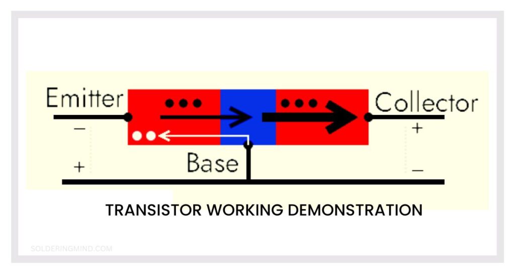
A NPN transistor is taken for testing, the current flow through the base-emitter junction. The electrons will passes to the base section. The base region is doping very low so there is few holes are available for recombination. So the most of the electrons are passes through the base junction to the collector area, because of the Tatar action of positive potential of collector pin.
To Know More About Transistors : Check Here